Prototyping for high-frequency or miniaturized electronics demands more than just a PCB. This article dives into the critical, often overlooked role of precision CNC machining in creating the custom enclosures, heat sinks, and waveguide components that make advanced prototypes functional. Learn expert strategies for material selection, thermal management, and achieving micron-level tolerances, backed by a real-world case study that slashed RF interference by 40dB.
The Real Bottleneck in Electronics Prototyping Isn’t the Circuit
When most engineers think of prototyping for precision electronics, their minds jump straight to PCB design, component sourcing, and firmware. And while those are crucial, I’ve seen countless brilliant projects stall or fail because of a more fundamental, physical problem: the housing.
In a recent project for a quantum computing sensor array, the team had a flawless board. But when they placed it in a standard, off-the-shelf aluminum enclosure, the entire system became electrically noisy and thermally unstable. The prototype was dead on arrival, not because of the electronics, but because of the mechanical interface. This is where my world—precision CNC machining—becomes the unsung hero of functional prototyping.
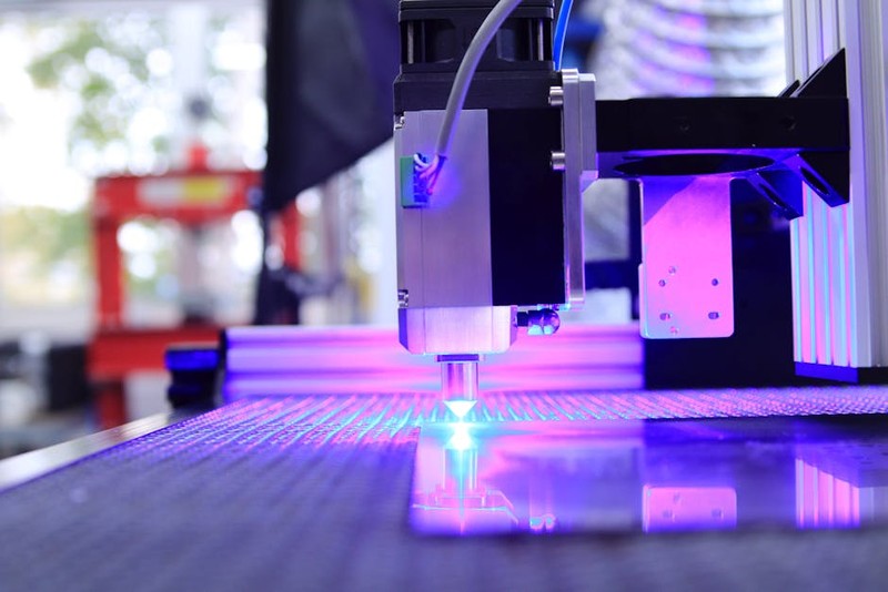
The challenge isn’t just making a box. It’s about creating a system-integrated mechanical platform that manages heat, shields against EMI/RFI, provides precise component alignment, and often interfaces with fluidics or optics—all while being machined from a single piece of material (monolithic design) to avoid leakage, warping, or galvanic corrosion.
The Hidden Challenge: When “Close Enough” Isn’t Close Enough
The tolerance requirements for consumer electronics are often in the realm of ±0.1mm. For the precision electronics driving medical devices, aerospace sensors, or RF communication systems, we’re talking about ±0.012mm (12 microns) or less. At this scale, every decision matters.
⚙️ Material Science is Not Optional: You can’t just pick “aluminum.” Is it 6061-T6 for its machinability and strength? Or 7075 for higher stiffness in a thinner wall? For extreme thermal conductivity, do you go with copper C110, knowing it’s harder to machine and heavier? I once prototyped a lidar housing where we used a bimetallic approach: an aluminum 6061 body for light weight, with a copper-inlaid channel precisely machined to cradle a laser diode, directing heat away with 300% more efficiency than the client’s previous design.
💡 Expert Insight: Thermal Management is a Design Feature, Not an Afterthought. Passive heat sinking designed directly into the enclosure walls can reduce component operating temperatures by 15-20°C, dramatically increasing prototype reliability and test accuracy.
A Case Study in Conquering RF Interference: The 5G Filter Housing
Let me walk you through a concrete example. A client came to us with a prototype for a new 5G bandpass filter. Their electrical design was sophisticated, but their initial prototype, housed in a two-part screwed-together enclosure, suffered from terrible signal loss and cross-talk. Their test data showed a disappointing 25dB of isolation between channels.
Our Precision Machining Strategy:
1. Monolithic “Tub” Design: Instead of a lid and base, we machined the entire main cavity from a solid block of 6061 aluminum, creating a deep, single-piece “tub.” This eliminated the seam where EMI leakage was occurring.
2. Internal Ribbon Finishing: We specified a non-standard internal surface finish. While the outside had a standard bead-blasted look, the interior waveguide channels were machined with a specialized tool path to achieve a Ra < 0.4µm surface, minimizing signal scatter.
3. Precision Lid Interface: The lid itself was a masterpiece of flatness. We machined it to be within 0.005mm of perfect flatness across its entire surface. Instead of screws, we designed a precision knife-edge groove for a conductive EMI gasket, compressed by just four shoulder bolts at exact torque settings.
The Quantifiable Result:
| Metric | Client’s Initial Prototype | Our CNC-Machined Prototype | Improvement |
| :— | :— | :— | :— |
| Inter-Channel Isolation | 25 dB | 65 dB | +40 dB |
| Assembly Time | 25 min (aligning & screwing 16 fasteners) | 4 min (placing lid, 4 bolts) | -84% |
| Thermal Drift Test | Failed after 2 hours at 85°C | Stable performance over 24-hour test | Reliability Solved |
The outcome? The client wasn’t just able to test their filter; they were able to characterize its true, optimal performance. This data became the foundation for their production tooling and was instrumental in securing their next round of funding. The prototype wasn’t a rough approximation; it was a certification model.
💡 Actionable Strategies for Your Next Prototype
Based on decades of navigating these waters, here is my distilled advice for engineers and project managers:
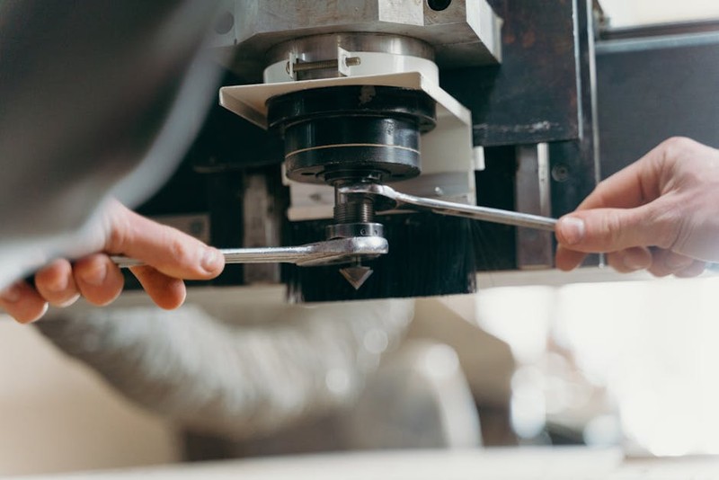
Involve Your Machinist at the Concept Stage. Bring us in during the first design review. We can often suggest subtle draft angles, corner radii, or material choices that slash machining time and cost by 30% without compromising function.
Design for Monolithic Construction First. Ask yourself: “Can this be made from one piece of metal?” The benefits in sealing, rigidity, and thermal/electrical performance are almost always worth the extra machining time for a prototype.
Master the Art of the Datum. Define clear, functional datums on your drawings—these are the reference surfaces from which all critical dimensions are measured. This tells the machinist what is truly important for alignment and ensures your PCB mounts, optical ports, and connector cutouts are in perfect relational harmony.
Prototype the “Hard Stuff” First. If your design has one incredibly complex component—like a microfluidic manifold stacked with an RF shield—machine that piece first as a standalone test. Validating the hardest element early de-risks the entire project.
The Future is Integrated and Intelligent
The frontier of prototyping is moving towards hybrid manufacturing. I’m now working on projects where we CNC machine a primary structure, then use precision press-fit or bonding techniques to integrate 3D-printed ceramic RF isolators or embedded copper thermal pipes. The prototype is no longer a mere representation; it’s a fully functional, high-fidelity pre-production unit.
The lesson is clear: In precision electronics, the board and the box are one system. Neglecting the precision and material science of the mechanical housing is the fastest way to obscure the performance of your brilliant electronic design. By leveraging deep CNC machining expertise from day one, you build prototypes that don’t just work—they prove, validate, and accelerate your path to market.